
TSMC Develops 0.42nm Interface for Next-Gen Transistors
TSMC and researchers create new interface for atomically thin transistors. Improved design for next-gen MoS2 transistors.
'%3E%3Crect%20width%3D'96'%20height%3D'96'%20fill%3D'%23B3261E'%2F%3E%3Ccircle%20cx%3D'30'%20cy%3D'24'%20r%3D'44'%20fill%3D'%23fff'%20opacity%3D'.12'%2F%3E%3Ccircle%20cx%3D'60'%20cy%3D'74'%20r%3D'40'%20fill%3D'%23000'%20opacity%3D'.10'%2F%3E%3C%2Fg%3E%3Cg%20fill%3D'%23fff'%3E%3Crect%20x%3D'29'%20y%3D'49'%20width%3D'8'%20height%3D'19'%20rx%3D'1'%2F%3E%3Crect%20x%3D'39'%20y%3D'40'%20width%3D'9'%20height%3D'28'%20rx%3D'1'%2F%3E%3Crect%20x%3D'50'%20y%3D'45'%20width%3D'8'%20height%3D'23'%20rx%3D'1'%2F%3E%3Crect%20x%3D'60'%20y%3D'53'%20width%3D'7'%20height%3D'15'%20rx%3D'1'%2F%3E%3Crect%20x%3D'41'%20y%3D'34'%20width%3D'5'%20height%3D'6'%2F%3E%3C%2Fg%3E%3C%2Fsvg%3E)
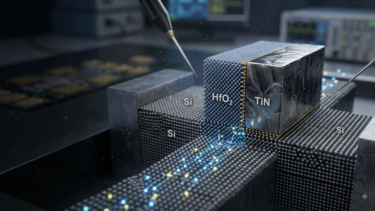
Researchers from National Yang Ming Chiao Tung University and Taiwan Semiconductor Manufacturing Company (TSMC) have made a significant breakthrough in the development of next-generation transistors.
They have successfully created a new interface design for atomically thin transistors, which is expected to improve the performance of these tiny devices.
The new interface design features a 0.42-nanometre aluminium oxide layer between monolayer MoS2 and a hafnium oxide dielectric. This extremely thin insulating layer helps the transistors maintain strong electrical control and carrier transport.
The development of this new interface design is a crucial step forward in the creation of next-generation transistors. Atomically thin transistors have the potential to revolutionize the field of electronics, enabling the creation of smaller, faster, and more efficient devices.
TSMC, a leading semiconductor manufacturing company, has been at the forefront of transistor technology development. The company's collaboration with researchers from National Yang Ming Chiao Tung University has led to this significant breakthrough.
The use of monolayer MoS2 in transistor design has been gaining attention in recent years due to its unique properties. MoS2 is a type of transition metal dichalcogenide that has excellent electrical conductivity and can be used to create ultra-thin transistors.
The development of this new interface design is expected to have a significant impact on the field of electronics. It is likely to enable the creation of smaller, faster, and more efficient devices, which will have a wide range of applications in fields such as computing, communications, and consumer electronics.
In conclusion, the development of this new interface design for atomically thin transistors is a significant breakthrough that is expected to have a major impact on the field of electronics. The collaboration between TSMC and researchers from National Yang Ming Chiao Tung University has led to this important development, which is likely to shape the future of transistor technology.
The breakthrough is a testament to the power of collaboration between industry and academia. It highlights the importance of investing in research and development to drive innovation and advance technology.
As the demand for smaller, faster, and more efficient devices continues to grow, the development of next-generation transistors is becoming increasingly important. The new interface design developed by TSMC and researchers from National Yang Ming Chiao Tung University is a significant step forward in this direction.
The future of transistor technology looks promising, with ongoing research and development expected to lead to even more breakthroughs in the coming years. The development of this new interface design is a significant milestone in this journey, and it is likely to have a lasting impact on the field of electronics.
In the long run, this breakthrough is expected to benefit consumers and industries alike, enabling the creation of smaller, faster, and more efficient devices that will transform the way we live and work.
The development of next-generation transistors is a complex task that requires ongoing research and development. However, with the collaboration between industry and academia, it is likely that we will see even more breakthroughs in the coming years.
The impact of this breakthrough will be felt across a wide range of industries, from computing and communications to consumer electronics. It is likely to enable the creation of devices that are smaller, faster, and more efficient, which will have a significant impact on our daily lives.
In conclusion, the development of this new interface design for atomically thin transistors is a significant breakthrough that is expected to have a major impact on the field of electronics. It is a testament to the power of collaboration between industry and academia and highlights the importance of investing in research and development to drive innovation and advance technology.
The future of transistor technology looks promising, and it is likely that we will see even more breakthroughs in the coming years. The development of this new interface design is a significant milestone in this journey, and it is likely to have a lasting impact on the field of electronics.
Frequently asked questions
What is the significance of the 0.42nm interface developed by TSMC?
The 0.42nm interface developed by TSMC is significant because it enables the creation of smaller, faster, and more efficient devices.
What is the role of monolayer MoS2 in transistor design?
Monolayer MoS2 is used in transistor design due to its unique properties, including excellent electrical conductivity and the ability to create ultra-thin transistors.